
Ceramic Printed Circuit Boards
As high-frequency electronic systems continue to evolve, ensuring optimal performance and reliability is key. Among the components that support these applications are ceramic printed circuit boards (PCBs). With their ability to efficiently transmit RF signals while maintaining signal integrity and minimizing loss, they provide a critical link in electronic devices like mobile communication equipment, radar systems, GPS units, and satellite communication platforms.
Compared to traditional organic substrates, ceramic printed circuit board are superior in several ways that make them the preferred choice for high-frequency applications. For example, their high thermal conductivity makes them ideal for dissipating heat generated by component traces and connections. They also exhibit good chemical stability, which is important for long-term operation.
In addition to these unique physical properties, a ceramic multilayer PCB supports complex circuit designs in compact form factors. Innovative techniques in layer stacking, via technologies, and precision alignment allow for finer traces and smaller components to be used, which in turn allows for higher densities and increased functionality in small form factors.
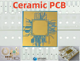
How Do Ceramic Printed Circuit Boards Handle High-Frequency RF Signals?
The process for fabricating a ceramic multilayer PCB begins with the design of the circuit using computer-aided design software. The layout must be considered for both function and aesthetics, taking into account factors such as signal integrity, electrical stability, and thermal management. Conductors and insulating layers are then added to the layout as necessary. Depending on the application, conductive materials may be applied by screen printing or inkjet printing. Vias, which connect the different layers of the ceramic substrate, are drilled using laser or mechanical drilling processes. Afterwards, the vias are filled with conductive and insulating pastes, which connect the various layers of the multilayer ceramic circuit board. Finally, the entire assembly is fired in a high-temperature furnace to sinter and fuse the conductive materials into a single ceramic substrate.
To ensure optimal RF signal transmission, it is important to take into account the length of the traces. If possible, it is best to avoid placing traces in parallel, as this can increase reflections and interfere with signals. If parallel traces cannot be avoided, they should be kept as short as possible. It is also important to ensure that the traces are properly matched with the driver and load. This helps to minimize impedance mismatches, which can lead to interference and loss of signal quality.
When selecting a manufacturer for your ceramic PCB, consider the company’s reputation and manufacturing capabilities. Ask for references or read reviews from other customers to gain insights into the company’s customer service and responsiveness, as well as its pricing structure and production lead times.
Once your RF PCB has been designed and manufactured, it is vital to perform tests to evaluate the overall performance and quality of the product. Common test methods include network analysis to measure S-parameters, time-domain reflectometry, and EMI/EMC testing. Other critical tests include thermal and power cycling. Lastly, it is essential to perform a thorough thermal and electrical inspection before the ceramic PCB is packaged and delivered for use in your application.